A team of Fraunhofer researchers has significantly enhanced the functionality of GaN power ICs for voltage converters: the researchers at Fraunhofer IAF integrated current and temperature sensors onto a GaN-based semiconductor chip, along with power transistors, freewheeling diodes and gate drivers. This development paves the way for more compact and efficient on-board chargers in electric vehicles.
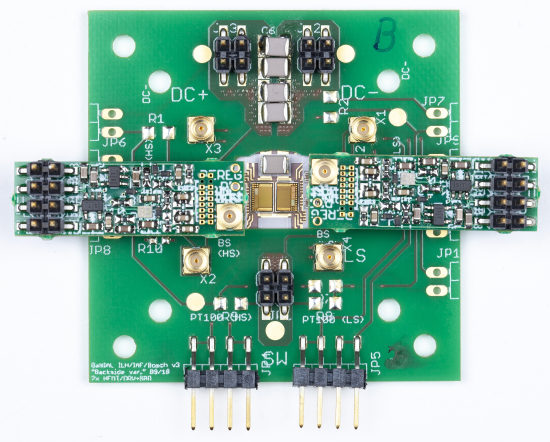
 The voltage converter shown is based on GaN power ICs measuring 4 x 3 mm². © Fraunhofer IAF
To make use of charging stations using alternating current, wall charging stations or conventional plug sockets where possible, users are dependent on on-board chargers. As this charging technology is carried in the vehicle, it must be as small and lightweight as possible, and also cost-efficient. It therefore requires extremely compact yet efficient power electronics systems such as voltage converters.
The Fraunhofer Institute for Applied Solid State Physics IAF has been conducting research on monolithic integration in the field of power electronics for several years. This requires several components such as power components, the control circuit and sensors to be combined on a single semiconductor chip. The concept makes use of the semiconductor material gallium nitride. Back in 2014, the researchers at Fraunhofer IAF succeeded in integrating intrinsic freewheeling diodes and gate drivers on a 600 V-class power transistor. In 2017, a monolithic GaN half bridge was then operated at 400 V for the first time.
The latest research results combine current and temperature sensors and 600 V-class power transistors with intrinsic freewheeling diodes and gate drivers in a GaN power IC for the first time.
As part of the GaNIAL (Integrated and efficient power electronics based on gallium nitride) research project, the researchers have provided functional verification of full functionality in a GaN power IC, achieving a breakthrough in the integration density of power electronics systems.
By additionally integrating sensors on the GaN chip, we have succeeded in significantly enhancing the functionality of our GaN technology for power electronics.
—Dr Patrick Waltereit, project manager of GaNIAL and deputy head of the Power Electronics business unit at Fraunhofer IAF
The GaNIAL project is funded by the German Federal Ministry of Education and Research; since 2016, this collaboration between Fraunhofer IAF and the BMW Group, Robert Bosch GmbH, Finepower GmbH and the University of Stuttgart has been working to develop powerful, compact GaN-based components for electromobility.
Compared to conventional voltage converters, the newly developed circuit simultaneously not only enables higher switching frequencies and a higher power density; it also provides for fast and accurate condition monitoring within the chip itself.
Although the increased switching frequency of GaN-based power electronics allows for increasingly compact designs, this results in a greater requirement for their monitoring and control. This means that having sensors integrated within the same chip is a considerable advantage.
—Stefan Mönch, a researcher in the Power Electronics business unit at Fraunhofer IAF
Previously, current and temperature sensors were implemented externally to the GaN chip. The integrated current sensor now enables feedback-free measurement of the transistor current for closed-loop control and short-circuit protection, and saves space compared to the customary external current sensors. The integrated temperature sensor enables direct measurement of the temperature of the power transistor, thereby mapping this thermally critical point considerably faster and more accurately than previous external sensors, as the distance and resulting temperature difference between the sensor and the point of measurement is eliminated by the monolithic integration.
The monolithic integration of the GaN power electronics with sensors and control circuit saves space on the chip surface, reduces the outlay on assembly and improves reliability. For applications that require lots of very small, efficient systems to be installed in limited space, such as in electromobility, this is crucial.
—Stefan Mönch
Mönch designed the integrated circuit for the GaN chip. Measuring just 4 x 3 mm², the GaN chip is the basis for the further development of more compact on-board chargers.
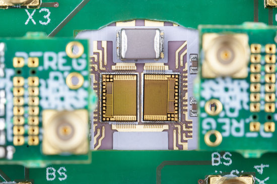
 GaN power ICs with integrated transistors, gate drivers, diodes and current and temperature sensors for condition monitoring. © Fraunhofer IAF
For the monolithic integration, the research team utilized the semiconductor material gallium nitride deposited on a silicon substrate (GaN-on-Si). The unique characteristic of GaN-on-Si power electronics is the lateral nature of the material: the current flows parallel to the surface of the chip, meaning that all connections are located on the top of the chip and connected via conductor paths.
This lateral structure of the GaN components allows for the monolithic integration of several components, such as transistors, drivers, diodes and sensors, on a single chip.
Gallium nitride has a further crucial market advantage compared to other wide-bandgap semiconductors, such as silicon carbide: GaN can be deposited on cost-efficient, large-area silicon substrates, making it suitable for industrial applications.
—Stefan Mönch


