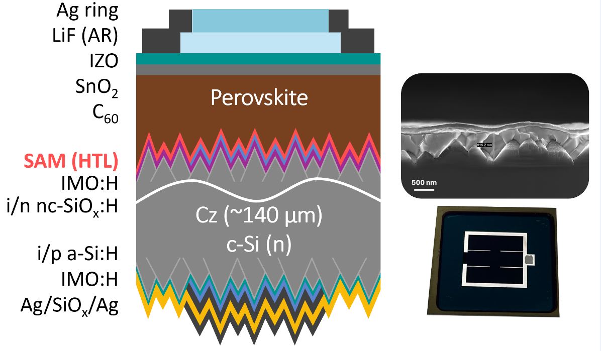
An international research team has developed a perovskite-silicon tandem solar cell that utilizes a bottom cell based on a heterojunction (HJT) design and improved hole transport layers (HTLs).
“The novelty of our approach lies in several innovative techniques and outcomes for advancing perovskite-silicon tandem solar cells,” the research's lead author, Angelika Harter, told pv magazine. “We enhanced the wettability of the perovskite layer and reduced shunting issues, which are common with conventional HTLs based on a phosphonic acid called methyl-substituted carbazole (Me-4PACz). This innovation leads to better film formation while maintaining the very good HTL characteristics of Me-4PACz.”
Furthermore, the research group used submicron-sized textured silicon bottom cells, which they say overcomes the challenges associated with traditional micrometer-sized textures. “These textures enable better integration of solution-processed perovskite films, reducing reflection losses and enhancing light in-coupling, while maintaining compatibility with industrial production methods,” said Harter.
Moreover, the scientists optimized the perovskite layer’s thickness and spin-coating parameters, which reportedly allows for efficient film formation on the submicron-textured surface and demonstrates the viability of using cost-effective and scalable solution-based methods for producing high-efficiency tandem cells. “The approaches used in this work are tailored to align with industrial manufacturing capabilities, such as the use of commercially available Czochralski silicon wafers. Showing here the compatibility with a solution-processed top cell, it also emphasizes the potential for upscaling possibilities,” Harter explained.
The academics presented the new cell design in the paper “Perovskite/Silicon Tandem Solar Cells Above 30% Conversion Efficiency on Submicron-Sized Textured Czochralski-Silicon Bottom Cells with Improved Hole-Transport Layers,” published in ACS Applied Materials & Interfaces, where they explained that they utilized a bottom HJT cell that was textured by wet-etching random pyramids to improve reflectance and passivation.
As for the perovskite film used in the top cell, they placed the Me-4PACz HTL combined with smaller PA molecules under the perovskite. “These additional PAs also allow the formation of more dipole-dipole interactions through hydrogen bridge bonding to adjacent phosphonic acid anchor groups,” the group explained. “The different PAs were diluted in ethanol (EtOH) and mixed with Me-4PACz (in EtOH) in a ratio of 1:4 and spin-coated on glass/ITO samples.”
The team built the tandem device with silver (Ag) metal contacts, passivating contacts made of silicon monoxide (SiOx), the bottom HJT cell, the proposed HTL, a perovskite absorber, electron transport layer (ETL) based on buckminster fullerene (C60) and tin oxide (SnO2), a transparent back contact made of indium zinc oxide (IZO), and a silver (Ag) metal contact.
“Having optimized the perovskite absorber fabrication for submicron textures, proof-of-concept tandems with the initial developments of the sequential application spin-spin-anneal of Me-4PACz with PAA enabled a champion device with a power conversion efficiency of 30.22% on a double-sided submicron-sized textured Cz-Si SHJ bottom cell achieving an open-circuit voltage of up to 1.954 V and a stabilized efficiency of 30.15%,” the researchers said.
“Overall, we demonstrate a high total short-circuit current density of 40.35 mA/cm2, which is remarkable considering the use of an industrially relevant silicon bottom cell with a thickness of only 140 μm and one of the highest reported for thin Cz material,” they added.
Looking forward, the research team said it intends to explore the use of sequential spin coating with an intermediate annealing step to further enhance the performance of the cell.