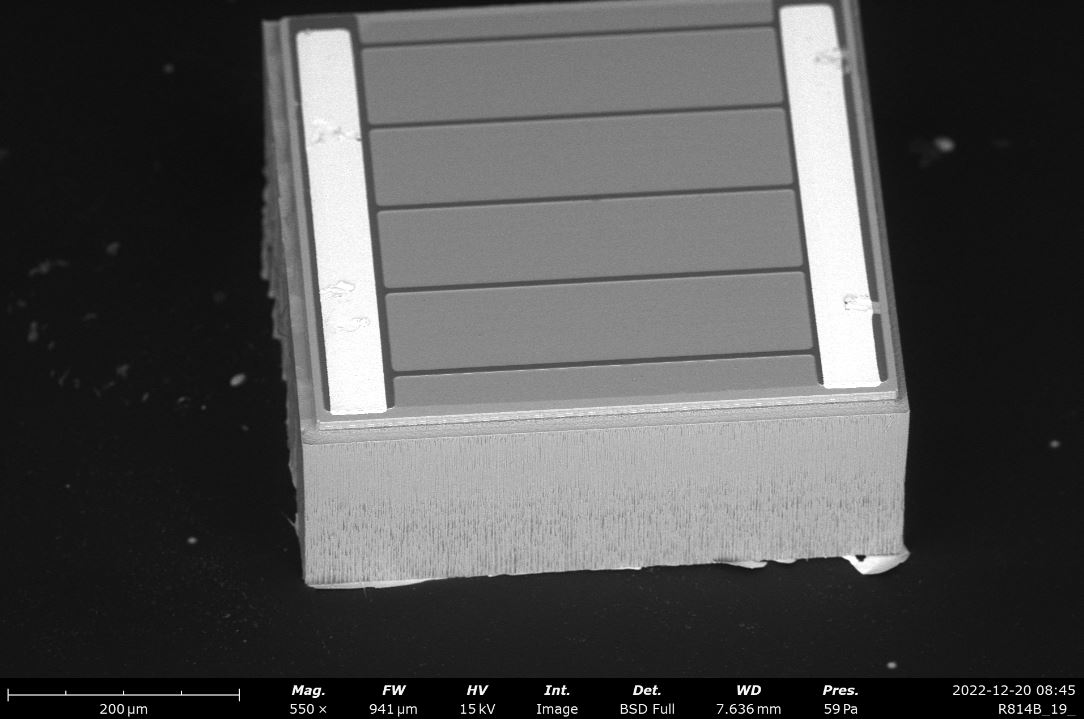
A Canadian research team has recently developed a micrometer-scale III-V solar cell for applications in concentrated photovoltaics (CPV).
Gallium arsenide (GaAs) and other III-V materials – named after the groups in the periodic table they belong to – are among the best known in terms of efficiency potential for solar cells. Their high production costs, however, have so far limited them to niche applications powering satellites and drones. In these devices, low weight and high efficiency are more pressing concerns than the cost of energy produced.
“The major drawback of these materials is their cost, typically more than two orders of magnitude more expensive than technology deployed on a large scale,” the scientists said. “To manage this problem, concentrated photovoltaic (CPV) technology promises to reduce costs by adding concentration optics to solar cells, thereby limiting the uses of III–V materials.”
The proposed solar cell is based on indium gallium phosphide (InGaP), indium gallium arsenide (InGaAs) and germanium (Ge) and has an active area of 0.25 mm2.
“Our solar cell achieved the highest open-circuit voltage for InGaP/InGaAs/Ge of different size in the literature to our knowledge,” the research's lead author, said Corentin Jouanneau. “The device also achieved a power conversion efficiency of over 30%.”
In the paper “Fabrication and characterization of high performance sub-millimetric InGaP/InGaAs/Ge solar cells,” published in Solar Energy Materials and Solar Cells, Jouanneau and his team explained that they build the cell with a metal contact made of nickel (Ni) and gold (Au), as well as with an antireflective layer relying on silicon nitride (SiN) and silicon oxide (SiO).
The use of plasma process enabled wafer losses of less than 10% and the design of complex shapes, the team noted. They used a process based on plasma etching for cell isolation and singulation, which reportedly enables to manufacture solar cells of any size and shape. As a result, they were able to produce cells with a size ranging from 12.25 mm to 0.01 mm and different shapes: round, triangular, maple leaf, hexagonal.
The cells were then tested under standard illumination conditions, and a 0.25 mm2 cell was found to be the champion device with an efficiency of 30.61% and a record-breaking open-circuit voltage of 2.39 V. This result was attributed to “excellent” sidewall passivation.
The smallest device, measuring only 0.01 mm2, was found to reach an efficiency of 21.40%.
“These cells were not manufactured for their performance but to demonstrate the capabilities of plasma etching,” the academics explained, noting that their work was mainly intended to identify the cells that were most affected by perimeter recombinations.
